
Imagine a tiny crystal so thin it’s almost two-dimensional, and inside it, tiny defects that glow like single stars. Now, imagine you could twist one layer of that crystal just a little, and watch those stars change color right before your eyes. Sounds like sci-fi? It’s not. This is the fascinating world of twist-tuned quantum emitters in hexagonal boron nitride (hBN).
- What Are Quantum Emitters in Hexagonal Boron Nitride?
- Why Does Twisting Layers Matter?
- How Does the Twist Angle Affect Emission Energy?
- Seeing the Twist Effect in the Lab
- What Controls the Size of the Shift?
- Why Not Strain or Other Effects?
- What Does This Mean for Quantum Technology?
- Challenges and Future Directions
- A New Twist on Quantum Light Control
You might think quantum emitters lock themselves in place, with nature fixing their light. But recent research shows that by mechanically twisting layers of hBN, you can actually control the color of light these quantum dots emit — all at room temperature. This breakthrough promises huge benefits for quantum technology and nanophotonics.
Let’s unpack how this works, why it matters, and what it means for the future of tiny light sources that could power quantum computers or ultra-secure communications.
What Are Quantum Emitters in Hexagonal Boron Nitride?
Quantum emitters are tiny defects inside crystals that trap electrons and emit light one photon at a time. In hBN, a crystal made of boron and nitrogen arranged in a hexagonal lattice, these defects create bright, stable single-photon sources at room temperature. That’s rare and valuable because most quantum emitters need ultra-cold environments to work.
Researchers study carbon trimers most often in hBN — groups of three carbon atoms that replace boron or nitrogen atoms in the lattice. These tiny imperfections create energy levels inside the bandgap of hBN, which allow electrons to jump and emit photons with specific colors. What’s remarkable is that these emitters shine brightly, remain stable, and researchers can engineer them with some control.
But here’s the catch: the light they emit depends heavily on their local atomic environment. If the surrounding atoms shift even slightly, the color of the emitted light can change. This sensitivity is what makes twisting layers of hBN so interesting.
Why Does Twisting Layers Matter?
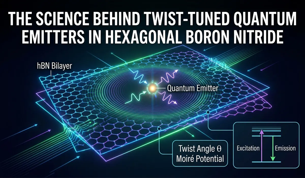
When you stack two layers of 2D materials like hBN, their alignment matters a lot. If you perfectly align them, the atoms sit one on top of another in a regular pattern. But if you twist one layer by just a few degrees, it creates a moiré pattern. This is a larger-scale interference pattern that changes the local atomic arrangement periodically.
This moiré superlattice isn’t just a pretty pattern; it changes the electronic environment at the interface between layers. Different stacking orders, like AA′, AB, or BA, create different local electric fields and atomic configurations. These changes can shift the energy levels of embedded quantum emitters.
Density functional theory (DFT) calculations show that the emission energy of carbon trimer defects varies nonlinearly with the twist angle. In some configurations, the emission shifts by up to 100 milli-electron volts (meV), which corresponds to a wavelength change of about 30 nanometers in the visible spectrum. That’s a huge shift for a single-photon emitter at room temperature.
How Does the Twist Angle Affect Emission Energy?
The twist angle, denoted as θt, controls the moiré periodicity — the size of the repeating pattern created by the twisted layers. Small angles (close to 0°) create large moiré cells, allowing atoms to rearrange and form domains of preferred stacking. Larger angles create smaller moiré cells, limiting atomic relaxation.
Each stacking configuration within the moiré cell affects the quantum emitter differently. For example:
- AA′ stacking is the natural bulk arrangement, alternating boron and nitrogen atoms vertically.
- AB and BA stackings break inversion symmetry, creating out-of-plane electric dipoles.
- These dipoles generate local electric fields that can shift the emission energy of defects.
DFT calculations reveal that at certain twist angles, the energy of the defect’s optical transition shifts significantly. But it’s not a simple linear relationship. The emission energy can increase or decrease depending on the local stacking and the exact position of the defect within the moiré supercell.
So, when you twist the top hBN layer, you’re effectively tuning the local environment of these quantum emitters, changing the color of light they emit.
Seeing the Twist Effect in the Lab
Theory is one thing, but can this be done experimentally? The challenge lies in mechanically twisting one hBN layer on top of another after stacking. Van der Waals forces usually lock the layers in place, making dynamic twisting difficult.
Researchers developed a clever method using a polymer stamp to pick up the top hBN flake, rotate it precisely, and place it back onto the bottom flake hosting the quantum emitters. This process can be repeated multiple times on the same sample, allowing in situ tuning of the twist angle.
Photoluminescence measurements show that the emission peak of single-photon emitters shifts by up to 30 nm as the twist angle changes. Some emitters blueshift, others redshift, and some show complex non-monotonic behavior. Importantly, the quantum nature of the emitters remains intact throughout the twisting process.
This experimental proof confirms that mechanical twisting is a viable way to control quantum emitters in hBN.
What Controls the Size of the Shift?
You might wonder why some emitters shift more than others. It turns out the distance of the emitter from the twisted interface matters a lot. Emitters right at the interface experience the strongest changes in their local environment, leading to larger shifts.
Also, the orientation of the emitter’s dipole plays a role. In-plane dipoles respond differently to out-of-plane electric fields created by certain stacking orders. This complexity means the emission tuning depends on the exact position and orientation of each defect.
Another factor is that the moiré superlattice’s electric potential decreases rapidly with distance from the interface, so emitters buried deeper in the crystal shift less.
Why Not Strain or Other Effects?
One might suspect that twisting could induce strain, which is known to shift emission energies in many materials. However, in this setup, the emitters are hosted in the bottom hBN flake, which remains unstrained during twisting. The top flake moves, but the bottom one does not experience significant strain.
Moreover, the observed shifts are too large to be explained by small strain effects alone. The local atomic environment change due to stacking order and moiré potential is a more plausible explanation.
What Does This Mean for Quantum Technology?
Controlling quantum emitters with a simple mechanical twist opens exciting possibilities. Imagine arrays of quantum dots whose emission colors can be tuned on demand, allowing synchronization or selective addressing in quantum circuits. This could lead to programmable quantum photonic devices integrated on chips.
Moreover, hBN’s ability to host bright, stable emitters at room temperature makes it practical for real-world applications, unlike many other quantum systems needing ultra-cold conditions.
The twist-tuning mechanism is also reversible and non-destructive, offering a flexible platform for experiments and devices.
Challenges and Future Directions
While the progress is impressive, challenges remain. Precise control over the position of emitters relative to the interface is still limited. Creating deterministic arrays of emitters with known twist-induced shifts requires advances in fabrication and imaging.
Also, better understanding the microscopic nature of defects and their interactions with moiré potentials will help refine control strategies.
Combining twist-tuning with other methods like electric gating or strain could unlock even richer control over quantum emitters.
A New Twist on Quantum Light Control
The discovery that twisting layers of hexagonal boron nitride can tune the emission of quantum emitters at room temperature is a remarkable leap. It shows how mechanical manipulation at the atomic scale changes the quantum world in ways we can harness.
This twist-tuned quantum emitter control adds a new dimension to the design of quantum photonic devices. It’s a reminder that even the tiniest shifts — a few degrees of twist — can have outsized effects.
For anyone fascinated by quantum technology or nanophotonics, this is a field to watch. The ability to program quantum light sources simply by turning a knob — or twisting a crystal — could redefine how we build quantum circuits.
If you’re curious about the future of light and quantum devices, keep an eye on twist-tuned quantum emitters in hexagonal boron nitride. The story is just beginning.
What is a quantum emitter in hexagonal boron nitride?
It is a defect inside hBN that traps electrons and emits single photons, acting as a tiny light source at room temperature.
How does twisting layers of hBN change the emission?
Twisting creates a moiré pattern that changes local atomic stacking, which shifts the energy levels of the defect and changes the color of emitted light.
Can the twist angle be changed after stacking?
Yes, using a special polymer stamp method, the top hBN layer can be mechanically rotated multiple times to tune the emission on the same sample.
How big is the shift in emission wavelength?
Shifts up to 30 nanometers (~100 meV) have been observed, which is significant for quantum emitters at room temperature.
Does twisting damage the quantum emitters?
No, the emitters remain stable and maintain their quantum properties throughout twisting.
Source: Adapted and synthesized from recent research on twist-controlled quantum emitters in hexagonal boron nitride, including density functional theory calculations and experimental photoluminescence studies.


